a4 size pcb layout Accepted file formats
If you are looking for PCB Layout Design Service - Medium Complexity ( 4 Layers ) | PCB Layout you've visit to the right place. We have 25 Pics about PCB Layout Design Service - Medium Complexity ( 4 Layers ) | PCB Layout like PCB Layout | PDF, Allegro PCB Design Solution Datasheet | Cadence and also What Are The Size & Shape Requirements For PCB Design? – PCB. Here it is:
PCB Layout Design Service - Medium Complexity ( 4 Layers ) | PCB Layout
 shop.nexpcb.com
pcb layers complexity nexpcb
PCB Design Guidelines - PCB Online S.r.l
 www.pcbdirectlab.com
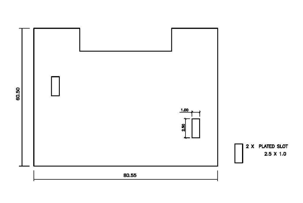
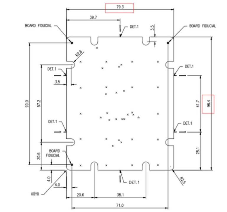
pcb mm ideally exact slots cutouts
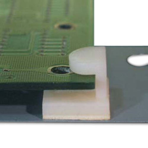
Adhesive PCB Spacers
 avt-connecting.com
pcb adhesive spacers spacer
How To Draw Pcb Layout From Circuit Diagram
 circuitlistadrienne.z13.web.core.windows.net
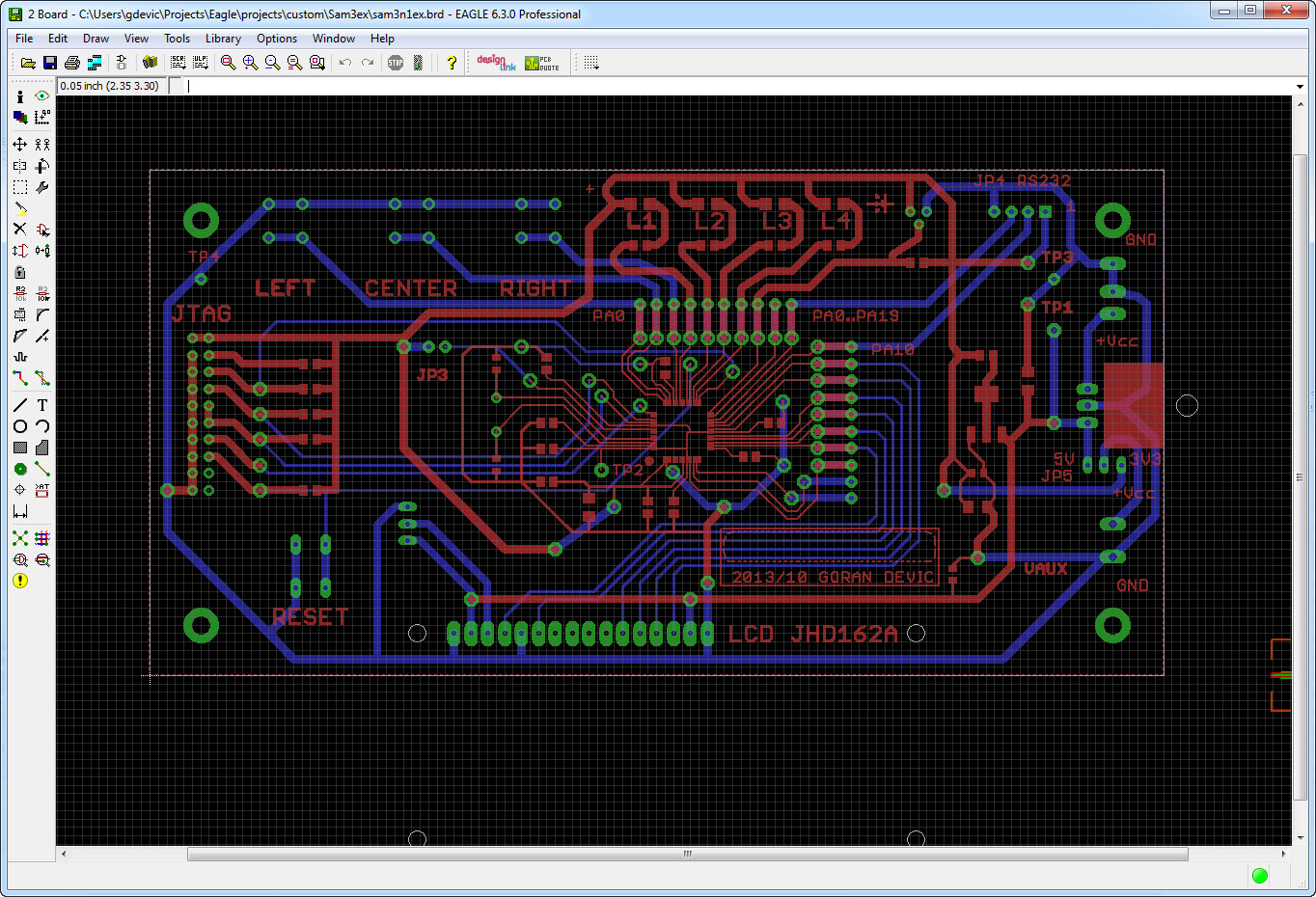
PCB Making: 4. Layout - Baltazar Studios
 baltazarstudios.com
layout pcb eagle making cad completed board
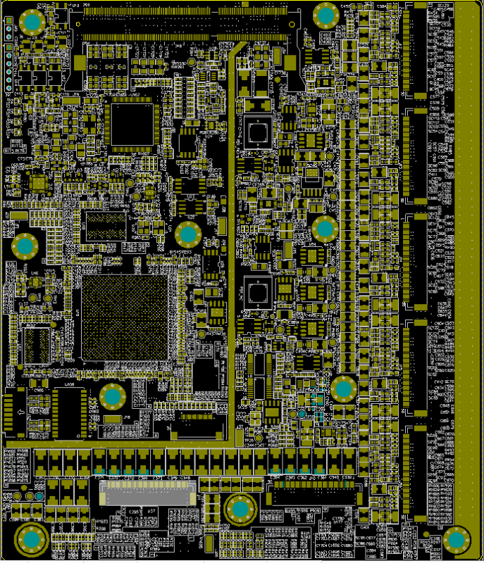
PCB Layout Design Service - High Complexity ( 6 Layers ) | PCB Layout
 www.nexpcb.com
pcb layers nexpcb complexity high
PCB Layout Design -HARDWARE - Share - PCBWay
 www.pcbway.com
pcb layout design package assign click ares numbers shown yes window below open save will
Pcb Hole Size Chart
 mavink.com
PCBWay 4-Layer PCB Stackup (October 2020) - PCB Artists
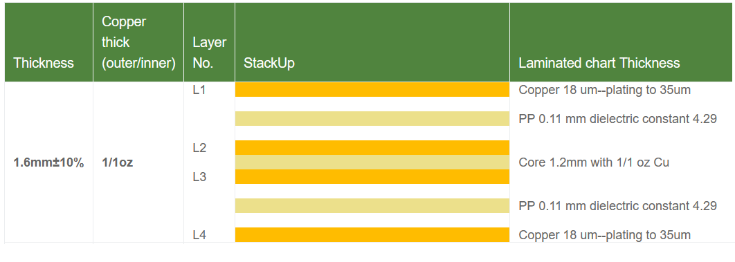 pcbartists.com
PCB Layout Design Best Practices - Developpa Electronics
 developpa.io
pcb determine minimum conductive ptr
Allegro PCB Design Solution Datasheet | Cadence
 www.cadence.com
Modular Display Project PCB Layout - EE12001
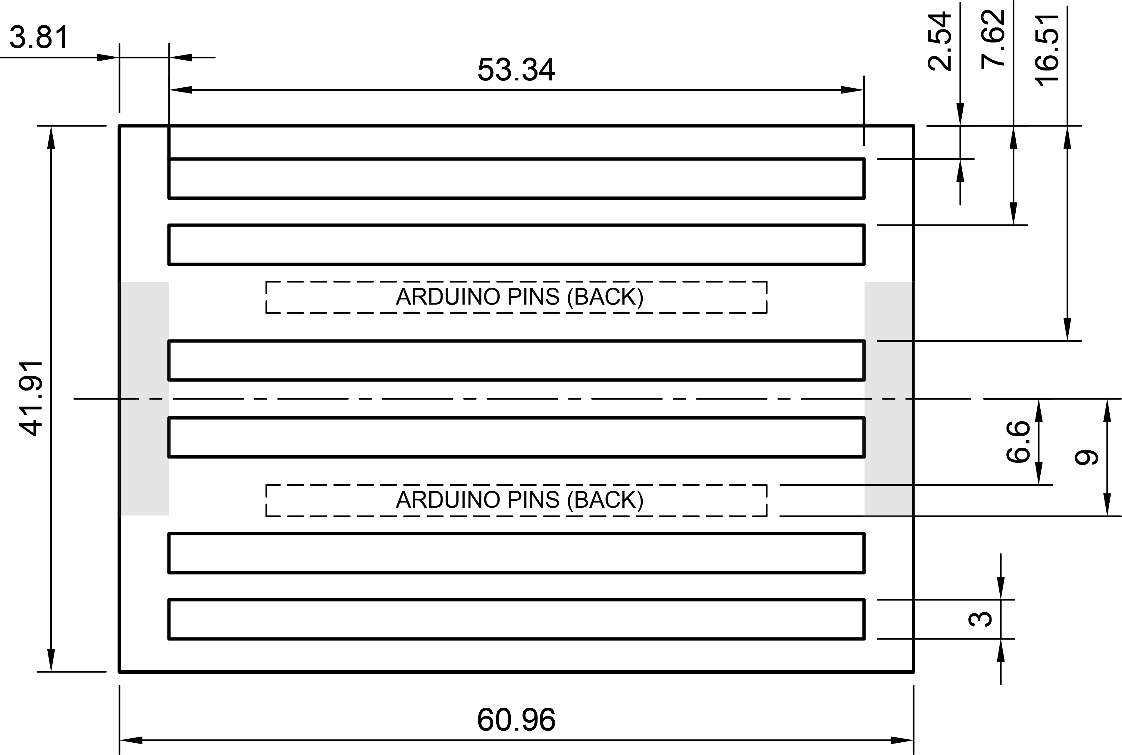 people.bath.ac.uk
PCB4YOU - Quality Pcb Layout At Reasonable Prices
 www.pcb4you.dk
pcb gerber relevant layers provide job standard library pdf
(PDF) PCB & Layout - DOKUMEN.TIPS
 dokumen.tips
Figure A.4: PCB Layout-Version 2 | Download Scientific Diagram
Complete Guide To PCB Layout Design: Tips, Basics, & Guidelines
 sfxpcb.com
LearnEMC - Introduction To Printed Circuit Board Layout For EMC
 learnemc.com
A4 Size PCB | A4 Size, Drilling Machine, Laminators
 www.pinterest.com
PCB Design Services - Electronic Circuit Board Layout
 at.pinterest.com
Pcb Design - 4 Layer PCB Layout With Microcontroller And IMU
 electronics.stackexchange.com
PCB Layout | PDF
 www.scribd.com
21+ Pcb Layout Design Rules Gambar Minimalis
 rangkaianampli.blogspot.com
Example Of Test Pcb Layout, Size 152 X 152 X 1.6 Mm | Download
 www.researchgate.net
What Are The Size & Shape Requirements For PCB Design? – PCB
 www.grande-pcba.com
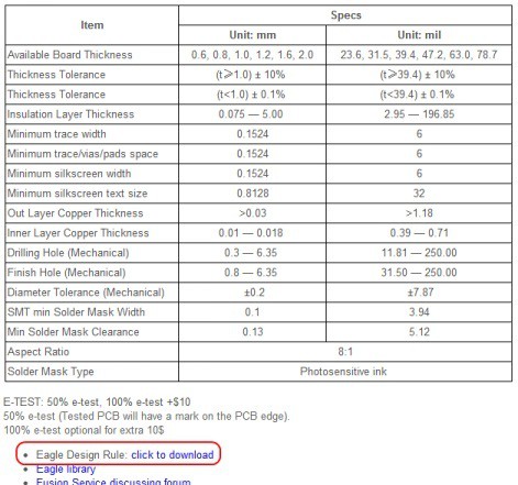
Accepted File Formats
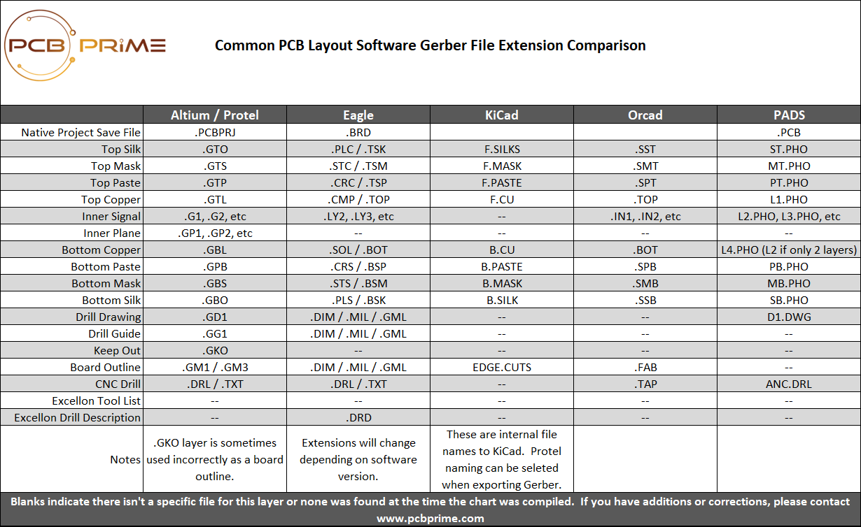 pcbprime.com
file formats accepted pcb tips drill cnc design
Pcb layout. Pcb making: 4. layout. Pcb layout design best practices