Circuit board layout guidelines for Class Pcb layout and pcb design services Pcb design and layout services
If you are searching about Printed Circuit Board (PCB) Design Service - CIRCUITSTATE Electronics you've visit to the right place. We have 25 Pictures about Printed Circuit Board (PCB) Design Service - CIRCUITSTATE Electronics like PCB Panel Design Guidelines 1 by Reliable China Circuit Boards, V4.0 PCB Design Typical Layout Characteristics | PDF | Printed Circuit and also Complete Guide to PCB Layout Design: Tips, Basics, & Guidelines. Here you go:
Printed Circuit Board (PCB) Design Service - CIRCUITSTATE Electronics
 www.circuitstate.com
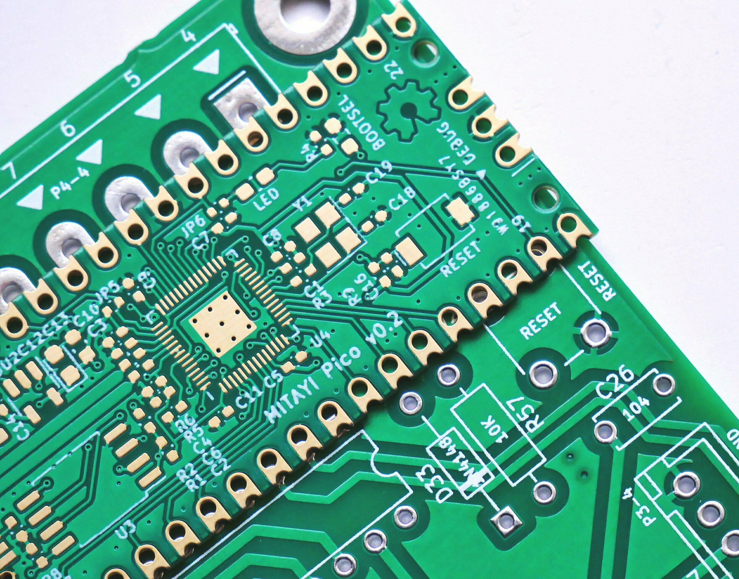
PCB Layout Guidelines For A Successful Design
 reversepcb.com
Custom PCB Board Design, PCB Layout Design Services, Electrical
 newchip.en.made-in-china.com
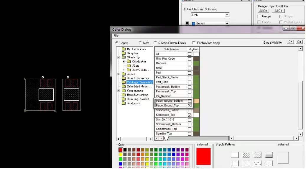
V4.0 PCB Design Typical Layout Characteristics | PDF | Printed Circuit
 www.scribd.com
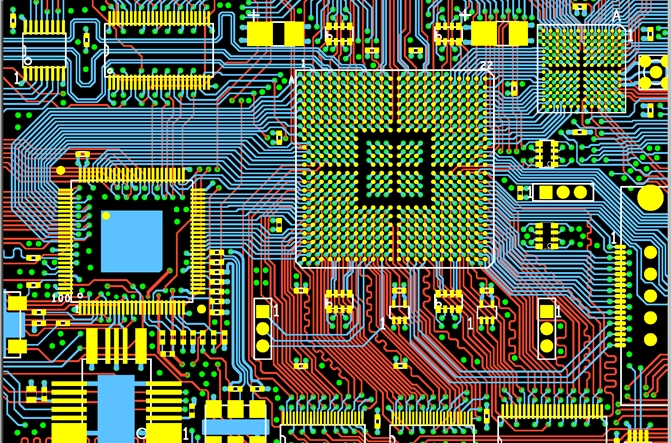
Main Design Guidelines & Layout Rules On High Speed PCB | Design
 www.pinterest.co.uk
Pcb Layout Guidelines For Design By PCBCART - Issuu
 issuu.com
PCB Layout Knowledge - Pcb Manufacturer China, Printed Circuit Board
 sfmpcb.com
Top 5 PCB Design Rules You Need To Know | PCB Design Blog | Altium
PCB Layout Design - RaceEL Systems
 www.raceelsystems.com
Custom PCB Board Design, PCB Layout Design Services, Electrical
 chenlu-pcb.en.made-in-china.com
SEM 1/2013: Circuit Design Part 2 : PCB Layout
 fypikhairiani.blogspot.com
PCB Layout Design In PCB Manufacturing
 pcbassemblymanufacturing.com
PCB - Design Guidlines PDF | PDF | Electronic Component | Printed
 www.scribd.com
Printed Circuit Board Design And PCB Layout Design Services
 www.embien.com
PCB Layout Services – Electronics Engineering Design Services
 www.microelectronicos.net
PCB Panel Design Guidelines 1 By Reliable China Circuit Boards
 www.scribd.com
Tips For PCB Layout Service - Engineering Your Ideas Into Reality
 gespcb.com
BASIC PCB Design Rules – Layout
 epci.eu
PCB Design And Layout Services - IBE
 www.pcbaservices.com
A Detailed Guide To PCB Layout Design – PCB HERO
 www.pcb-hero.com
Mastering PCB Layout Design Rules For Optimal Circuit Performance - 86PCB
 86pcb.com
Pcb Design Layout Guidelines Pcb Layout Guidelines For Design
 pcbways.pages.dev
Unlocking Success: Dominating PCB Layout Design Rules - 86PCB
 86pcb.com
Pcb Design - PCB Layout Of A Circuit - Electrical Engineering Stack
 electronics.stackexchange.com
Complete Guide To PCB Layout Design: Tips, Basics, & Guidelines
 sfxpcb.com
A detailed guide to pcb layout design – pcb hero. Pcb layout knowledge. Basic pcb design rules – layout