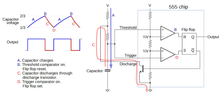
inside a 555 timer 555 timer ic die inside teardown chip tiny world package most popular ne555 pins penny venerable shots analysis electronics ken Circuits using 555 timer
If you are searching about 555 timer teardown: inside the world's most popular IC you've came to the right web. We have 25 Pics about 555 timer teardown: inside the world's most popular IC like 555 timer teardown: inside the world's most popular IC, 555 Timer Teardown - Electronics-Lab and also Learn about 555 timer IC pin configuration, working & operating modes. Read more:
555 Timer Teardown: Inside The World's Most Popular IC
 www.righto.com
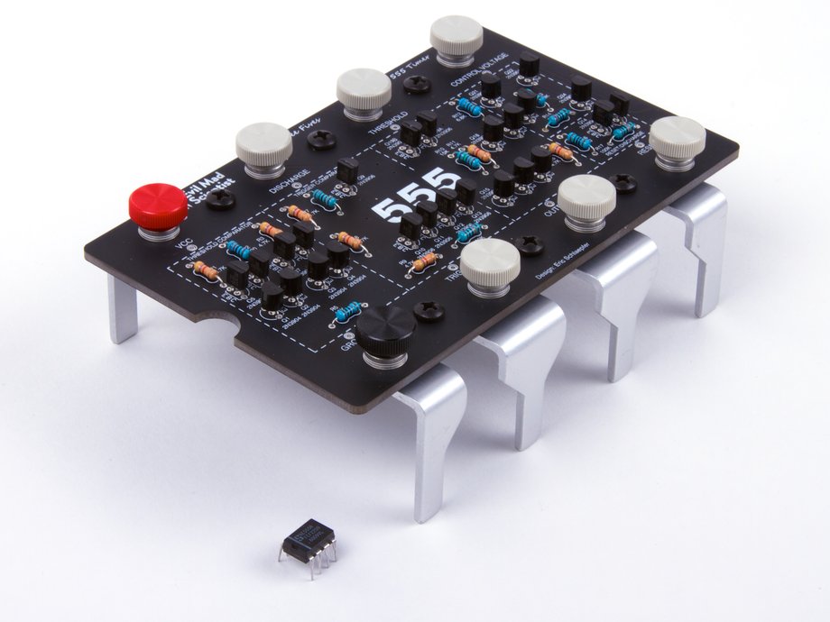
555 timer ic kit mad scientist evil inside discrete ne555 fives three teardown lab created working size large most diagram
555 Timer Teardown: Inside The World's Most Popular IC
 www.righto.com
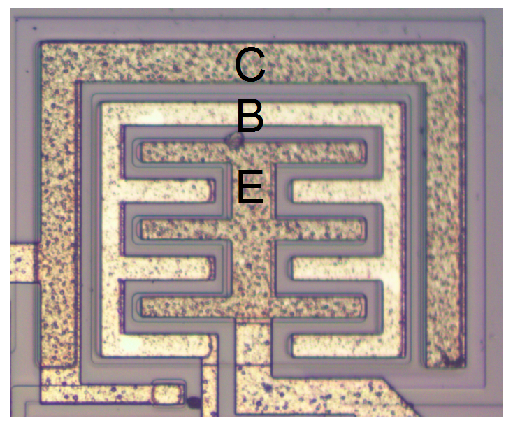
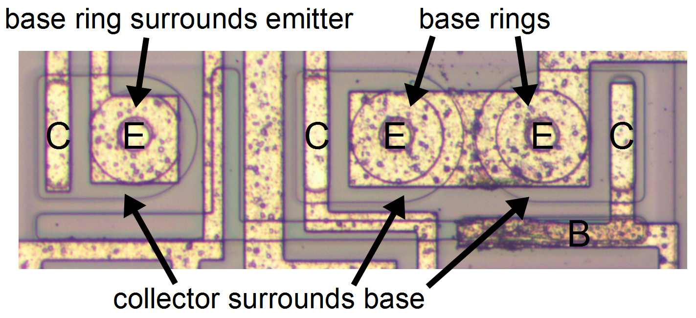
timer transistor teardown npn labeled large collector emitter output base current high inside chip
555 Timer Teardown: Inside The World's Most Popular IC
 pic-microcontroller.com
timer cmos teardown explained engineered explanation brief adafruit
555 Timer Teardown: Inside The World's Most Popular IC
 www.righto.com
555 timer ic shirriff hackaday
555 Timer Teardown: Inside The World's Most Popular IC
 www.righto.com
timer transistor teardown npn silicon labeled collector chip emitter base inside doped along ic
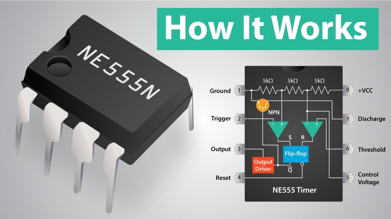
Learn About 555 Timer IC Pin Configuration, Working & Operating Modes
 playwithcircuit.com
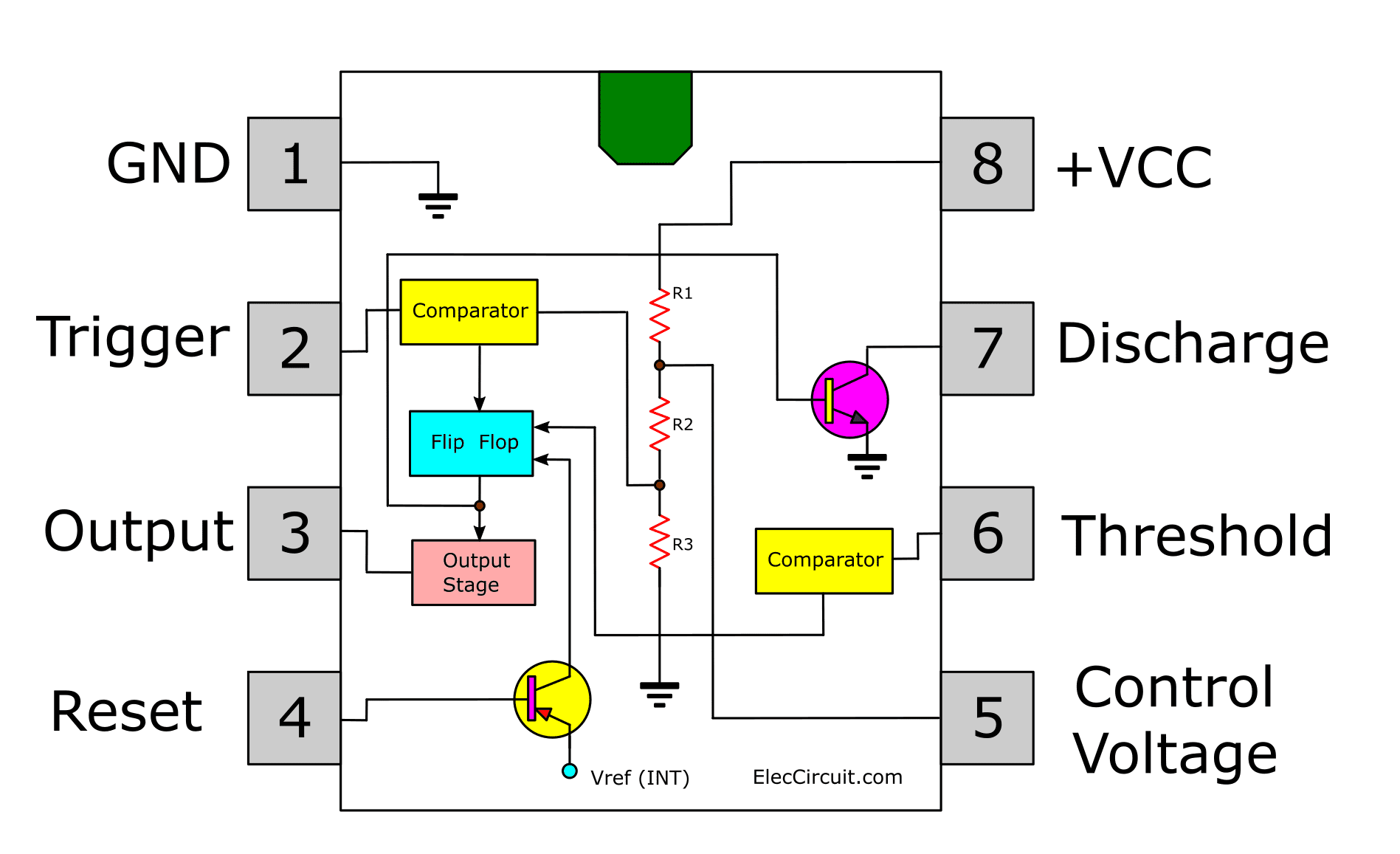
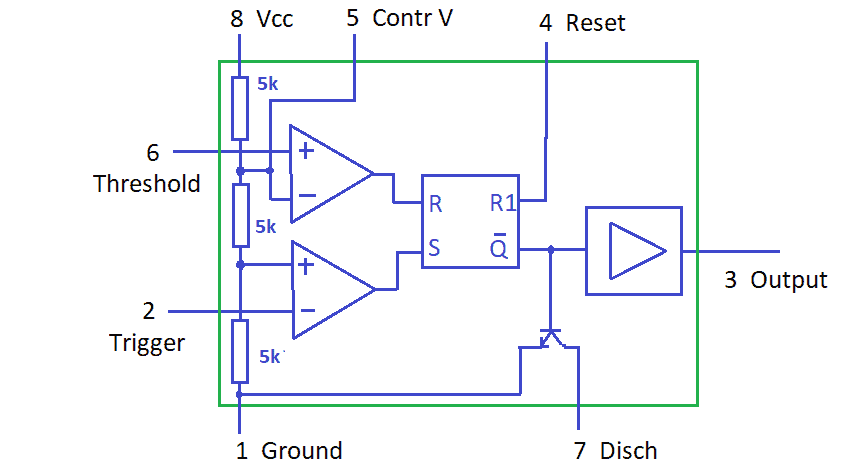
Explain The Functional Block Diagram Of Ic 555 Timer 555 Tim
 schematicgartenbrq.z21.web.core.windows.net
Functional Block Diagram Of Ic 555 Timer 555 Timer Diagram I
 manualpiulador4fk.z14.web.core.windows.net
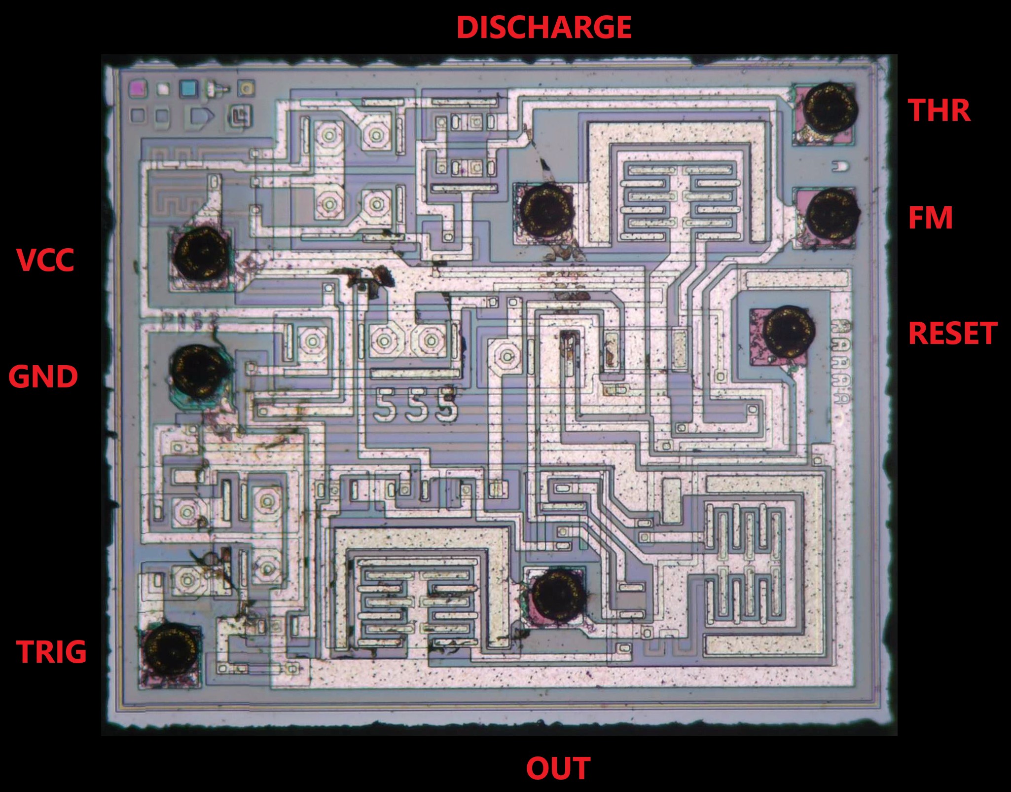
Inside A 555 Timer
 guidemanualdigger.z21.web.core.windows.net
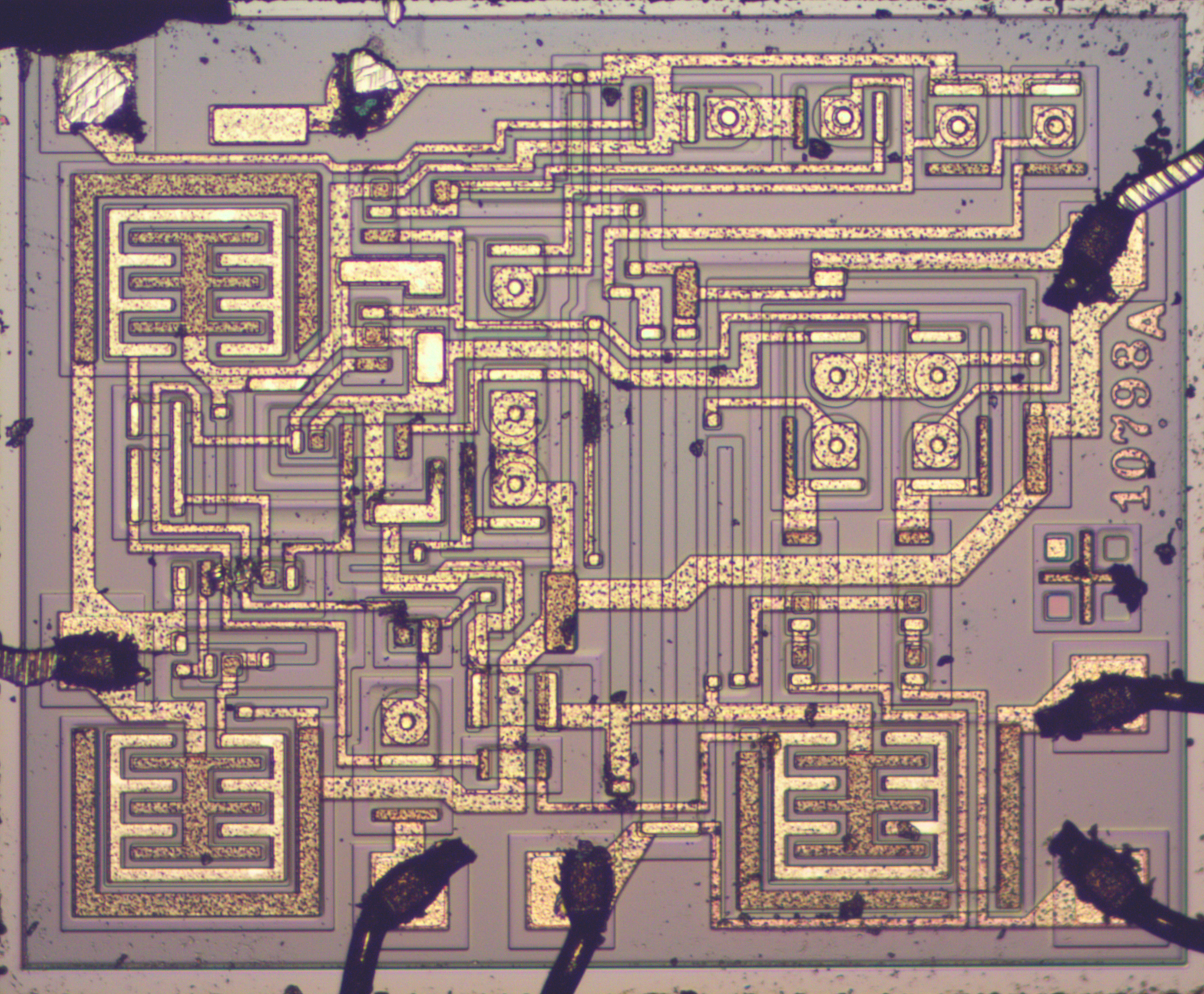
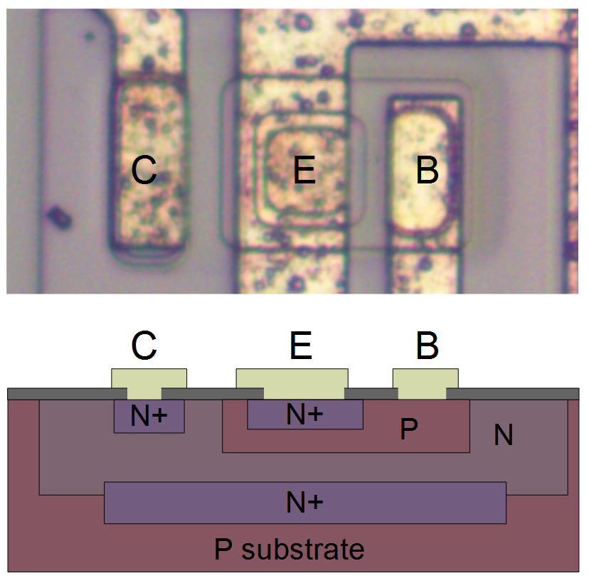
Silicon Die Teardown: A Look Inside An Early 555 Timer Chip - Jpralves.net
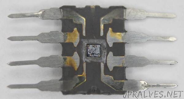 jpralves.net
Ic 555 Schematic Circuits Using 555 Timer
 nistneernetganschematic.z21.web.core.windows.net
555 Timer Teardown: Inside The World's Most Popular IC
 www.righto.com
timer transistors teardown mirror inside current form three two blog share venerable shots die emitters chip base same they adafruit
Silicon Die Teardown: A Look Inside An Early 555 Timer Chip, 52% OFF
 informacionpublica2021.svet.gob.gt
Silicon Die Teardown: A Look Inside An Early 555 Timer Chip, 45% OFF
 ricardoalpoim.com.br
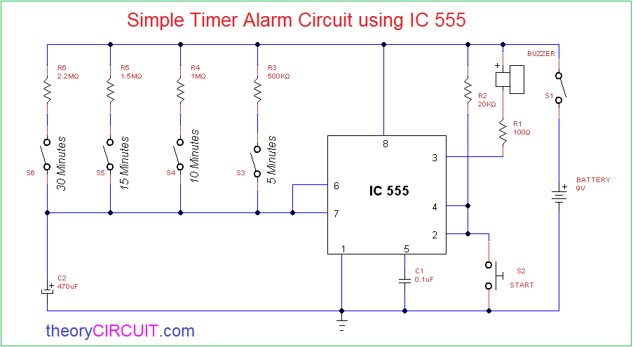
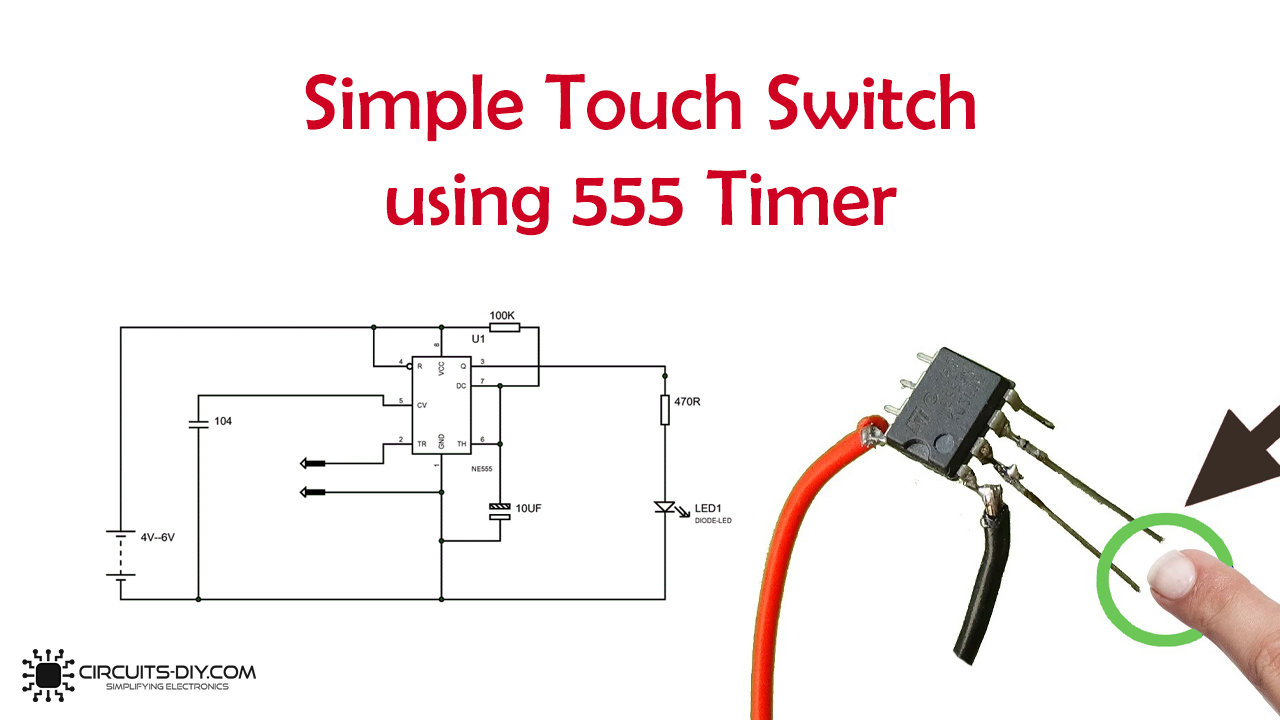
Circuits Using 555 Timer
 spusiasepcfcwire.z21.web.core.windows.net
The 555 Timer | Tiny Transistors
 www.tinytransistors.net
timer thomson stmicroelectronics semiconductor largest
Silicon Die Teardown: A Look Inside An Early 555 Timer Chip, 45% OFF
 boys.velvet.jp
Silicon Die Teardown: A Look Inside An Early 555 Timer Chip
 www.righto.com
Electronics 555 Timer Tutorial
 stormus570circuit.z21.web.core.windows.net
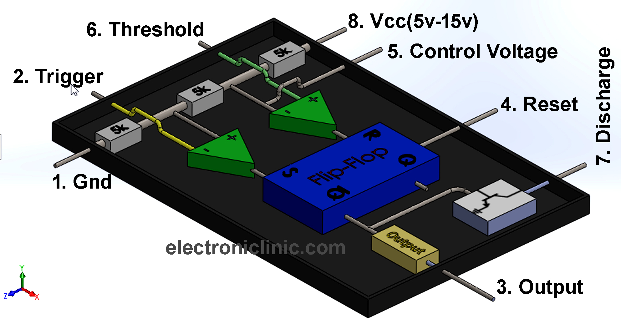
555 Timer IC Working, Pin Diagram, Examples (Astable, Monostable, Bistable)
 www.electroniclinic.com
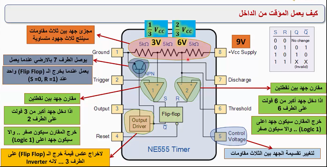
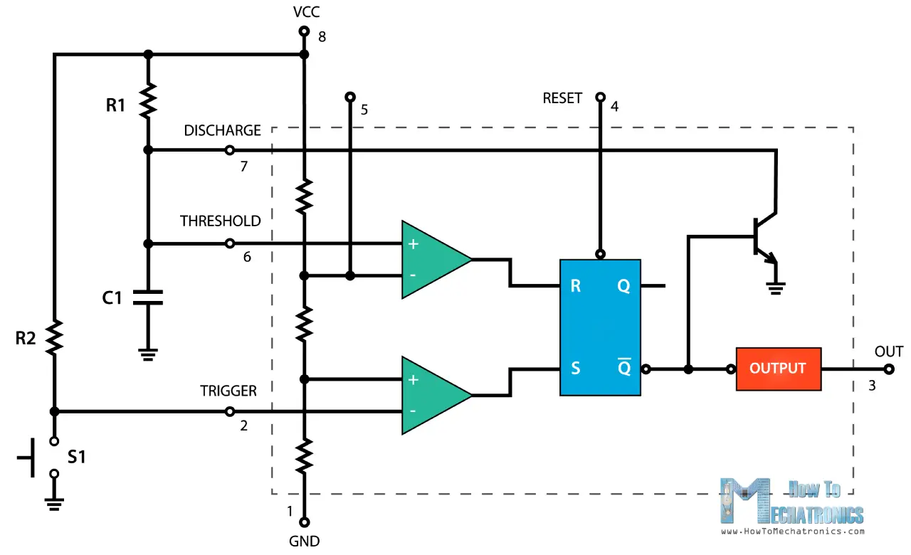
التصميم الالكتروني (36) دائرة المؤقت 555 من الداخل - Inside 555 Timer
 qelectronicdesigns.blogspot.com
Circuit Diagram 555 Timer
 wirelealtoeconsulters.z21.web.core.windows.net
555 Timer Teardown: Inside The World's Most Popular IC
 www.righto.com
timer can package metal teardown ic inside banana scale eight
555 Timer Schematic Symbol - Wiring Diagram And Schematics
 www.caretxdigital.com
555 Timer Teardown - Electronics-Lab
 www.electronics-lab.com
555 timer teardown die inside ic penny electronics popular lab venerable shots most february analysis blog tiny package tag pins
The 555 timer. Silicon die teardown: a look inside an early 555 timer chip, 45% off. 555 timer schematic symbol