LPDDR4 Design and Layout Tutorial Lpddr4 pcb layout guidelines Ddr3l/ lpddr4/ ddr4 phy ip
If you are looking for Figure 1 from Multi-standard low-power DDR I/O circuit design in 7nm you've came to the right place. We have 25 Pictures about Figure 1 from Multi-standard low-power DDR I/O circuit design in 7nm like Usb 2 0 Pcb Layout Guidelines - Design Talk, Ddr4 Pcb Layout Guidelines - Uppress and also Ddr Pcb Layout Guidelines. Here it is:
Figure 1 From Multi-standard Low-power DDR I/O Circuit Design In 7nm
 www.semanticscholar.org
Ddr3 Routing Guidelines And Routing Topologies - Diysica
 diysica.blogspot.com
LPDDR4 Design And Layout Tutorial - ADVANCED PCB Design Rules - YouTube
 www.youtube.com
Nine Dot Connects » Altium Designer PCB Editor, Nine Dot Connects, 9dot
 www.ninedotconnects.com
LPDDR4 Simulation Environment Construction. A The Layout Of The
 www.researchgate.net
DDR4 And LPDDR4 - Board Design Verification And Challenges - Mentor
 www.mentor.com
ddr4 lpddr4 verification counterparts pcb
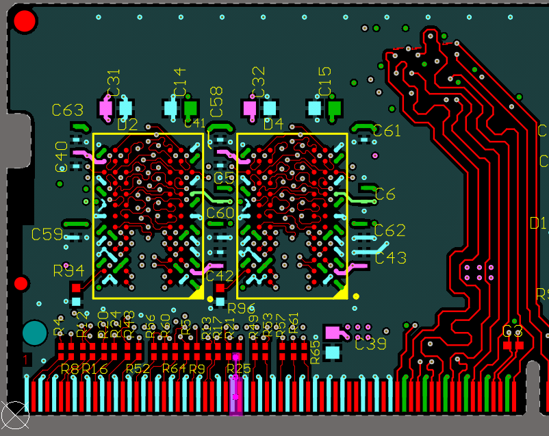
TDA4vM LPDDR4 Layout - Processors Forum - Processors - TI E2E Support
 e2e.ti.com
lpddr4 e2e 6mil 8mil ca0 3mil processors
Simulation VIP For LPDDR4 | Cadence
 www.cadence.com
Usb 2 0 Pcb Layout Guidelines - Design Talk
 design.udlvirtual.edu.pe
(PDF) Jacinto 7 LPDDR4 Board Design And Layout Guidelines (Rev. B
 pdfslide.net
LPDDR4 Design Für PCB Entwickler - Zuken GmbH
 www.zuken.com
LPDDR4 Design Für PCB Entwickler - Zuken GmbH
 www.zuken.com
LPDDR4 PCB Layout Guidelines | Zuken EN
 www.zuken.com
Ddr Pcb Layout Guidelines
 lessonlibrarypanaches.z13.web.core.windows.net
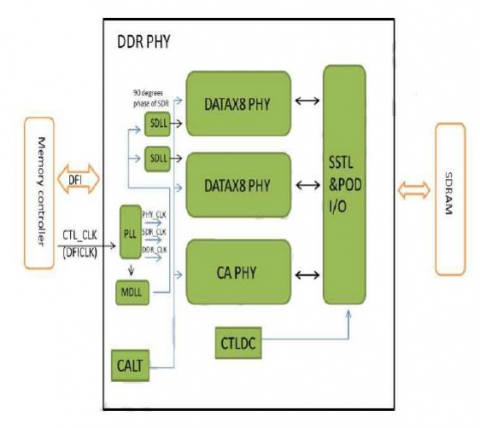
DDR3L/ LPDDR4/ DDR4 PHY IP - 1866Mbps(在 UMC 28HPC+ 中经过硅验证)
 cn.design-reuse.com
Nine Dot Connects » DDR3, DDR4, LPDDR4 Design And Layout Services, Nine
 www.ninedotconnects.com
layout ddr3 design services ddr ddr4 double
Versal: PCB Layout Rules For 2x32 LPDDR4 Pin Efficient
Nine Dot Connects » Altium Designer PCB Editor, Nine Dot Connects, 9dot
 www.ninedotconnects.com
Ddr4 Pcb Layout Guidelines - Uppress
 uppress4.blogspot.com
DDR4 PCB Layout: Best Practices For Optimal Performance – Hillman
 hillmancurtis.com
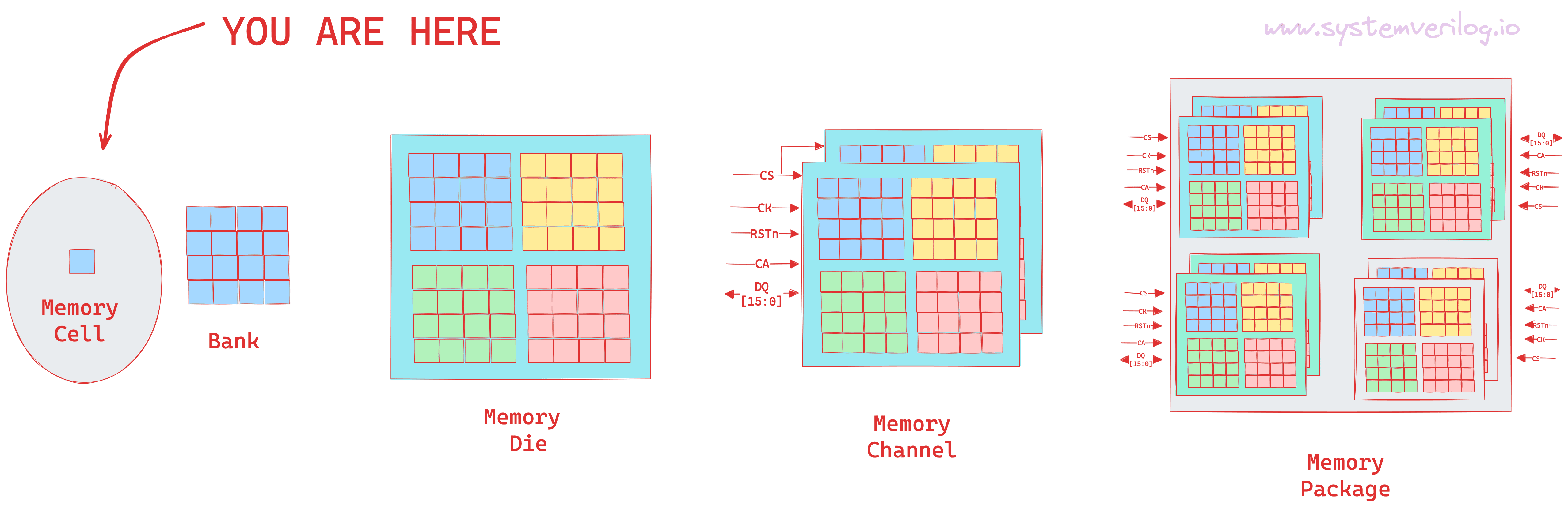
LPDDR5 Tutorial - Deep Dive Into Its Physical Structure - Systemverilog.io
 www.systemverilog.io
PCB Routing Guidelines For DDR4 Memory Devices And Impedance | Blog
 resources.altium.com
LPDDR4 PCB Design And Layout Tutorial - LPDDR4 Length Matching - YouTube
 www.youtube.com
Stm32 Lpddr4 Schematic Design
 mavink.com
LPDDR5 Tutorial - Deep Dive Into Its Physical Structure - Systemverilog.io
 www.systemverilog.io
Ddr4 and lpddr4. Usb 2 0 pcb layout guidelines. Lpddr5 tutorial