PCIe in PCB Design: Layout and Routing Guidelines High speed printed circuit board (pcb) design guidelines – pcb hero 10 automotive pcb design guidelines
If you are searching about PCB Routing Guidelines for DDR4 Memory Devices and Impedance | Blog you've came to the right place. We have 25 Pictures about PCB Routing Guidelines for DDR4 Memory Devices and Impedance | Blog like High Speed Printed Circuit Board (PCB) Design Guidelines – PCB HERO, High Speed Printed Circuit Board (PCB) Design Guidelines – PCB HERO and also 11 Best High-Speed PCB Routing Practices | Sierra Circuits. Read more:
PCB Routing Guidelines For DDR4 Memory Devices And Impedance | Blog
 resources.altium.com
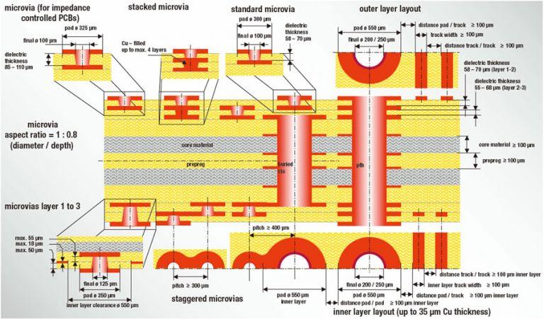
HDI PCB Design Guidelines For Manufacturing
 www.hemeixinpcb.com
hdi pcb guidelines processing rules
High Speed Pcb Design And Layout, Expert PCB Design Service [ With Step
 www.venture-mfg.com
pcb design speed high autodesk layout circuits step courtesy guide
The Best High Speed Board Design Guidelines | NWES Blog
 www.nwengineeringllc.com
usb pcb routing interfaces phy connectors requires controlled impedance
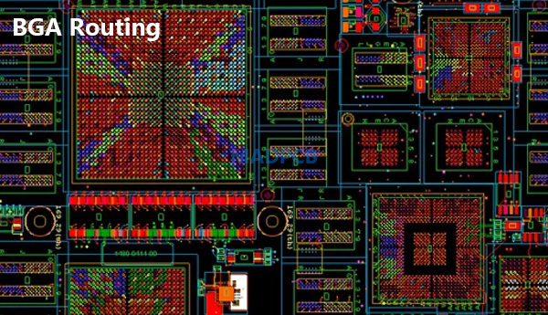
BGA Routing Guidelines In Complex PCB Layout Design | MADPCB
 madpcb.com
11 Best High-Speed PCB Routing Practices – PCB HERO
 www.pcb-hero.com
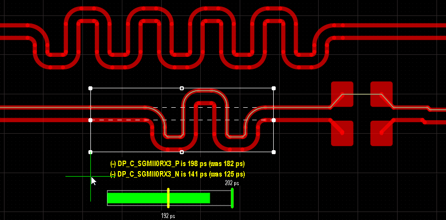
Secrets Of Differential Pair Routing In High-Speed PCB Design | NWES Blog
 www.nwengineeringllc.com
PCB Routing - My Site
 www.geekyedge.com
pcb routing high might also like
11 Best High-Speed PCB Routing Practices – PCB HERO
 www.pcb-hero.com
Pcb Design Layout Guidelines Pcb Layout Guidelines For Design
 pcbways.pages.dev
The Digital Engineer's Guide To RF PCB Design Guidelines: Layout And R
 www.pcb-hero.com
PCB Layout Guidelines For High Speed Applications - HardwareBee
 hardwarebee.com
pcb guidelines electronic speed
11 Best High-Speed PCB Routing Practices | Sierra Circuits
 www.protoexpress.com
Ddr Pcb Layout Guidelines
 worksheetdbgambs.z19.web.core.windows.net
10 Automotive PCB Design Guidelines | Sierra Circuits
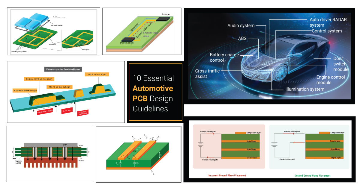 www.protoexpress.com
PCB Design Guidelines For EMI EMC - RayMing PCB
 www.raypcb.com
High Speed Printed Circuit Board (PCB) Design Guidelines – PCB HERO
 www.pcb-hero.com
High-Speed PCB Design Guidelines
 circuits-diy.com
pcb circuits techniques diy absolute soldering practices anas ejaz 1843
High Speed Pcb Layout Guidelines - Design Talk
 design.udlvirtual.edu.pe
High Speed USB Design Guidelines - EEWeb
 www.eeweb.com
routing
High Speed Pcb Layout Guidelines - Design Talk
 design.udlvirtual.edu.pe
High Speed Routing Guidelines For Advanced PCBs | PCB Design Blog
 resources.altium.com
speed high guidelines routing core advanced credit pcbs pcb can union system top processing unions upgrades conversions design altium ranks
Switched-Mode Power Supply PCB Layout Guidelines | Altium
 huiwenedn.com
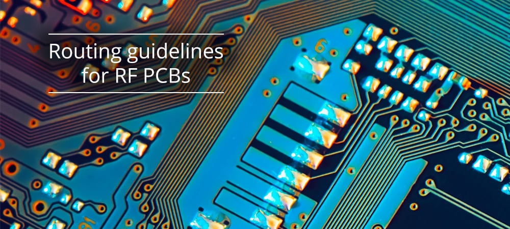
Routing Guidelines For RF PCBs
 www.proto-electronics.com
rf routing pcb enrutamiento pcbs leiterplatten hf proto directrices
High Speed Printed Circuit Board (PCB) Design Guidelines – PCB HERO
 www.pcb-hero.com
Pcb routing. High-speed pcb design guidelines. Pcb layout guidelines for high speed applications