kumpulan skema layout pcb Pcb design tips and challenges A professional custom pcb design, pcb layouts and circuit design
If you are searching about PCB Design Services - Electronic Circuit Board Layout you've visit to the right place. We have 25 Images about PCB Design Services - Electronic Circuit Board Layout like Simple PCB Layout Design: Tips and Strategies | Cadence, Complete Guide to PCB Layout Design: Tips, Basics, & Guidelines and also Top 10 Tips for Efficient PCB Layout Design | 911EDA. Read more:
PCB Design Services - Electronic Circuit Board Layout
 at.pinterest.com
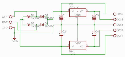
Inspirasi Skema Layout Pcb Bbe, Skema Pcb
 pulsalistrikd.blogspot.com
Teknik Pembuatan Layout PCB Secara Manual | PDF
 id.scribd.com
Complete Guide To PCB Layout Design: Tips, Basics, & Guidelines
 sfxpcb.com
PCB Design & PCB Layout : A Guide To Design The Right PCB
 www.hemeixinpcb.com
pcb
A Professional Custom PCB Design, PCB Layouts And Circuit Design | Upwork
 www.upwork.com
Pcb Layout Design Image Download – Artofit
 www.artofit.org
PCB Layout Design – Twinkle Technology
 twinkle.com.my
pcb layout twinkle
Foto Aplikasi Buat PCB Layout
 www.viva.co.id
Pcb Layout Design Image Download – Artofit
 www.artofit.org
Pcb Design - PCB Layout Of A Circuit - Electrical Engineering Stack
 electronics.stackexchange.com
SEM 1/2013: Circuit Design Part 2 : PCB Layout
 fypikhairiani.blogspot.com
Pcb Layout Design Image Download – Artofit
 www.artofit.org
Pcb Layout Design Image Download – Artofit
 www.artofit.org
Learn Pcb Design & Layout Techniques - SoftArchive
 sanet.st
Pcb_layout - EasyEDA Open Source Hardware Lab
 oshwlab.com
Design Pcb Schematics And Layout For Your Projects By Koksalkurt
 www.fiverr.com
pcb schematics screen
Top 7 PCB Layout Design Tips & Best Practices For Beginners
 circuits-diy.com
pcb beginners practices
Top 10 Tips For Efficient PCB Layout Design | 911EDA
 www.911eda.com
PCB Design Service Singapore | Schematic To Board Layout
 www.pic-control.com
Inspirasi Skema Layout Pcb Bbe, Skema Pcb
 pulsalistrikd.blogspot.com
Simple PCB Layout Design: Tips And Strategies | Cadence
 resources.pcb.cadence.com
18 PCB Layout Tips For Improving Your PCB Design And Reducing
 camptechii.com
pcb design layout trace tips spacing traces manufacturing headaches board copper side out ground between pads using each opposite improving
285 Gambar Pcb Layout Terbaik | Rangkaian Elektronik, Desain Tata Letak
 www.pinterest.com
pcb layout kon
Diagram Skema Dan Lay-Out PCB | PDF
 id.scribd.com
Pcb layout design image download – artofit. Diagram skema dan lay-out pcb. Learn pcb design & layout techniques